Boot ROM
According to the Allwinner V3s datasheet, the integrated boot system consists in a 32KB boot ROM mapped at addresses 0xffff0000-0xffff7fff, that can boot from SPI NOR Flash, SPI NAND Flash, SD Card and USB.
In Allwinner terminology, this boot ROM is called "BROM" (for "Boot ROM") or "eGON.BRM" (for "Embedded GO-ON Bootloader Boot ROM", who knows what this means exactly?).
But in another place in the same datasheet, it is stated that it can boot from eMMC, too.
Wrong!
We found that the available information is either incomplete, inacurate, misleading or completely false.
What triggered our suspicion was this first mismatch and the lack of details regarding the boot process: not a single explanation on the boot firmware format and/or exact location.
The original v3s_lichee.zip SDK is not very helpful in this regard.
Hopefully, as Allwinner tends to use a rather consistent similar boot process for all its SoCs, the lichee-v2.0.tar.gz from Olimex is actually giving some clues, albeit it does not mention the V3s.
But the best source of information on the Allwinner chips is certainly the sunxi community, that is dedicated to gather information around the Allwinner SoCs.
And although it describes in details the Allwinner A10/A20 and A31 chips and not the V3s, their BROM page is a golden mine.
The A20-V1.2.tar.gz SDK from Olimex is also relevant, as it contains some original source code for the Allwinner A20 SoC bootloader.
Eventually, in order to clear all doubts regarding the Boot ROM role, we had to reverse-engineer the Allwinner V3s Boot ROM by disassembling its source code. The current findings are available in our repository, in the "brom.s" file, with our comments added:
https://github.com/FunKey-Project/Allwinner-V3s-BROM
Power-On Reset (POR)
As it is common to all ARM Cortex-A architecture CPUs, the Allwinner V3s fetches the first instruction to execute from the first 32-bit word in a vector table located at address 0xffff0000.
On the V3s, this location is the first 32-bit word in the Boot ROM, that contains as its first vector a branch instruction to the reset function", located immediately after the vector table.
And except for the irq vector that contains a branch instruction to the first-level routine handling interrupt request, all other standard ARM vectors only contain a branch to a "forever loop" as they are not implemented at this stage.
Note
A non-standard "FEL" vector is appended at the end of the vector table.
This provides an indirect way to access the FEL code, allowing to change its actual location while keeping the ability to address it using a fixed location.
Reset Function
The reset function is the first useful piece of code executed on the CPU.
At this point, the only known-working hardware is the CPU 24 MHz clock derived from the external crystal, the CPU itself and its internal registers which may not even be initialized.
Register Initialization
This is the role of the short reset function that clears all CPU registers (except r0 that is set to 1) and jumps to the actual BROM header first 32-bit word.
BROM Header
The BROM location contains a "BROM header" structure made up of:
-
a 32-bit word branch instruction that jumps to the
startfunction -
an ASCII magic signature "eGON.BRM"
-
a header length in bytes (32)
-
a boot version in ASCII ("1100" for version 1.1.00)
-
an eGON version in ASCII ("1100" for version 1.1.00)
-
a platform information in ASCII ("1681" for the V3s)
-
a 32-bit word padding
Start Function
The start function role is to setup a minimal execution environment with a call stack, using the internal static RAM A1 and C memory.
BROM Output Pin Toggling
We found that the first step of the start function consists in toggling an unidentified "BROM Output" pin.
This guess is based on the fact that, according to the H6 User Manual which has a register with similar offset (0xa4) in its system configuration block, it is indeed BROM_OUTPUT_REG, and its bit 0 is BROM_OUTPUT_ENABLE, and bit 1 is BROM_OUTPUT_VALUE.
Tip
If this pin is actually available, this would allow to check with an oscilloscope if the CPU is running or not, but we were not able to locate it.
Multi-CPU Check
The second step in the start function is to check for multi-CPUs. This is unlikely to do anything, as the V3s only contains a single CPU, but the code is probably here for compatibility with other multi-core SoCs.
Start CPU #0
The third step in the start function is to initialize the CPU #0 operating mode:
-
define the system as an ARMv4+ architecture
-
set the CPU #0 in SVC (supervisor) mode
-
disable both normal IRQ and fast FIRQ interrupt requests
-
set the system as little-endian
Disable Memory Access Features
The next step in the start function is to disable all kind of memory access optimization features:
-
disable the MMU
-
disable the data cache (D-Cache)
-
disable the program flow prediction and the instruction cache (I-Cache)
Disable Watchdog
The next step in sequence in the start function is to disable the watchdog.
Tip
However, this is described in the datasheet as having "no effect"?
It may be a write-once capability that is disabled when written anything but zeros.
Configure Internal System Bus Clocks
The clocks for the AHB1 (Advanced High-speed Bus #1) and APB1 (Advanced Peripheral Bus #1) bus clocks are set up to enable access to most of the internal peripheral controllers, except UART, TWI that are on APB2 bus and EMAC and USB that are on AHB2 bus, as can be seen in the diagram below:
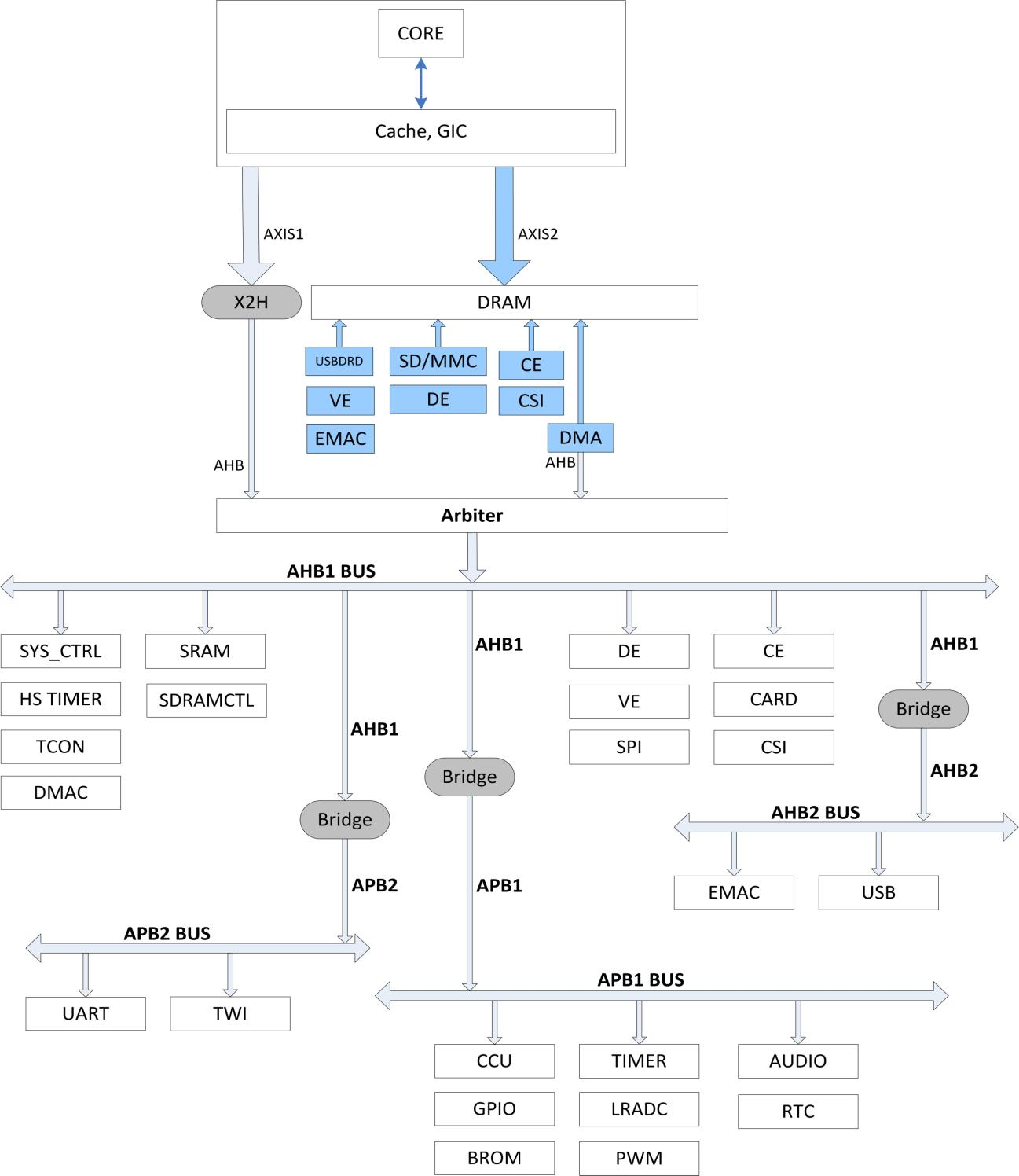
Bug
In the above diagram taken from the datasheet, the BROM looks like is located on the APB1 bus, which is certainly not possible, as the system already accesses it before enabling its clock!
Initialize DMA and PIO
In the next step in the start function:
-
the DMA engine is enabled
-
the PIO (Peripheral I/O) controller is enabled to access external pins
-
the DMA engine is reset
Initialize Stack Pointer in SRAM A1
At this stage, the 16KB SRAM A1 is available at addresses 0x00000000-0x00003fff, so a first stack pointer is initialized at the top of SRAM A1 memory.
Resume from Standby Mode
A check is then performed to see if the CPU is resuming from standby mode.
Hint
This standby mode is not documented anywhere!
If yes, a jump to the resume_from_standby function is done, where further checking is performed on the resume header:
-
check for a "eGON.BT0" signature at an address
0x01f01da8that is suspected to be a "standby resume entry address register" -
check if the resume address the follows the signature is valid (if its 10 MSB bits are all zeros)
-
verify the header checksum
If all these checks passed, the resume entry point is called, otherwise a call to the boot function is performed to try to resume the normal boot sequence.
Bug
However, the normal boot sequence will not be able to continue, as the next steps to enable the SRAM C block are skipped, so this is expected to fail!
Enable SRAM C
In the next to final step of the start function, the SRAM C (44 KB) is enabled at addresses 0x00004000-0x000efff:
-
first, an undocumented register in System Control block is cleared, that is suspected to enable SRAM C access to the CPU and the DMA
-
Then the Video Engine (VE) is started by enabling its clock and reseting it. It is suspected that the reason it is done here is because the SRAM C block is tied to the Video Engine function
Initialize Stack Pointer in SRAM C
In the last step of the start function, the stack pointer is set 4KB below the end of SRAM C (address 0x0000dffc), before calling the final boot function.
Boot Function
The role of the boot function is to implement the boot sequence described in the datasheet:
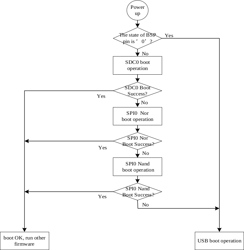
Wrong!
However, we found out that this diagram is inacurate!
Check UBoot Button
The first step in the boot function is to check if an "UBoot button" is pressed by calling the check_uboot function.
Note
Here, "UBoot" stands for "USB Boot", it has nothing to do whith "Das U-Boot" bootloader!
However, as the check_uboot function uses a special register to check the input pin rather than the standard PIO controller, it is not possible to determine from the code which pin is actually involved.
We are not aware of any pin on the V3s that has this capability, although we suspected the PF6 pin (pin 100) to have this function as it has no alternate function like all the other pins, but this is not the case: pulling this pin to GND during the boot process has no effect, so likely, this function is not implemented on the V3s.
If this hypothetical button is pressed during the boot sequence, the boot function would branch directly to the FEL USB Boot code, bypassing the normal boot process.
Boot from Flash Memory
Unlike what is describe in the control flow diagram above, the V3s search order for the Flash memory to boot from is actually the following:
-
SD Card on SDC0 interface
-
eMMC chip on SDC2 interface
-
SD Card on SDC2 interface
-
NOR Flash chip on SPI interface
-
NAND Flash chip on SPI interface
For all Flash memory types, the boot process is similar:
-
read one 512 byte block at address
0x00000000from the Flash device to get a "BOOT0 Header" -
check the "eGON.BT0" signature at the very beginning of the loaded block using the
check_magicfunction (example for booting from MMC0) -
check the length field at offset 16: the second stage bootloader length must be < 32KB (0x8000), example for booting from MMC0
-
check if the length field bits 24:31 are null (which is always true anyway because of the test above, example for booting from MMC0)
-
perform 2 attempts to read the required number of 512-byte blocks for the specified length and load them at address
0x00000000from the Flash device (it looks like the first block is re-read, example for booting from MMC0). The reason to perform 2 attempts is unknown -
eventually, jump to the
.boot_splfunction, which:-
loads
0xfcinto register r1 and0x0into register r0 -
calls the
jump_splfunction that: -
saves the r0 contents to r4
-
calls in turn the
jump_tofunction that:- loads r0 into the program counter and never returns, actually launching the loaded SPL (Secondary Program Loader) at address
0x00000000in SRAM A1 and C
- loads r0 into the program counter and never returns, actually launching the loaded SPL (Secondary Program Loader) at address
-
If no bootable Flash memory is found, the boot function will branch to the FEL USB Boot code.
Booting from SD Card
As on the FunKey S the only available Flash memory to boot from is the SD Card, we will focus on this one and ignore the other devices.
The only SD Card specificity regarding the boot process is that the BOOT0 header above is fetched from 2 byte-offsets from the beginning of the card:
The reason why these particular offsets were chosen is unknown, but they are not very convenient for card following a standard partitioning scheme:
-
the 8KB offset falls in the middle of the Primary GPT in a GUID Partition Table scheme. As most SD Card are optimized in hardware for the old MBR scheme, it is not critical
-
both offsets fall within the first 1GB on the disk, which is most of the time not allocated for disk partitions, so they require specific tools to access them
On the FunKey S, the 8KB offset is used for the SPL, detailed in the next section.
The SD Card interface used (0 or 2) is stored into the BOOT0 header in the byte at offset 40, and bit 5 in this byte is set to 1 when the BOOT0 header is loaded from offset 128 KB, and to 0 when booted from offset 8KB by this code.
FEL
The FEL is a low-level subroutine also contained in the BootROM on Allwinner devices. It is used for initial programming and recovery of devices using USB.
The FEL is actually implementing a tiny USB stack for a proprietary USB protocol different from the standard DFU (Device Firmware Update) protocol used by many other devices.
Using some specific tools on the host computer, it is possible to read or write data to/from the device over USB and execute code on it, providing a way to boot the system over USB.
These "sunxi-tools" are described here and here.
Warning
For the V3s, it is mandatory to build the version from the repository, as the versions packaged in the different operating systems are too old and do not take into account the V3s chip.
Using the "sunxi-tools" and the built-in FEL mode from the BootROM, it is possible to boot the V3s CPU over USB without any attached Flash storage.