PMIC
From the previous section, we can summarize the V3s power supply requirements to:
- SMPS for +3.3V / 1.2A for the I/O power supply
- LDO for +3.3V_AO / 30 mA for the Always-On power supply (RTC timer)
- LDO for +3.0V / 200 mA for the analog power supply
- SMPS for +1.8V / 1A for the DDR2 DRAM power supply
- SMPS for +1.25V / 1.6 A for the core power supply
On the LicheePi Zero board used in our FunKey Zero prototype, a triple SMPS EA3036 is used for generating these +3.3V, +1.8V and +1.2V voltages, with an additional XC6206 LDO for the +3.0V (the +3.3V Always On is connected directly to +3.3V). Although compact (the EA3036 is a tiny 3 mm x 3 mm QFN20 package), this solution is not ideal as it does not provide a battery charger and monitoring capability, which is a requirement for the FunKey S device.
PMICs
As it is generally the case with such a complex SoC requiring multiple voltages, high current and proper voltage sequencing, all major manufacturers provide dedicated companion chips called PMICs (Power Management Integrated Circuits), in charge of these tasks. Allwinner is not an exception through its sister company X-Powers.
Their AXP20x products are highly-integrated PMICs that are optimized for applications requiring single-cell Li-battery (Li-Ion/Polymer), multiple output DC-DC converters and LDOs. Here is a block diagram:
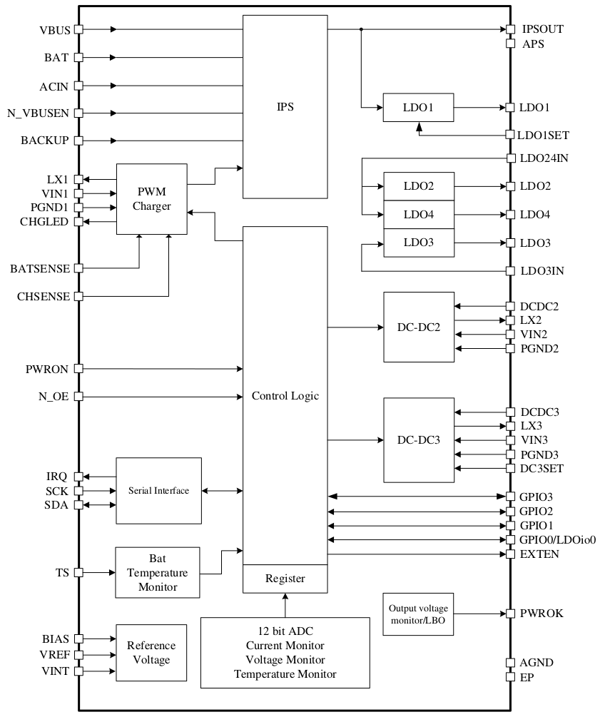
The AXP20x features:
-
A wide choice of input power source, the best source is output as IPSOUT inside the IPS (Intelligent Power Select) block:
-
USB VBUS
-
Battery BAT
-
ACIN wall plug (not used in the FunKey S)
-
BACKUP battery (not used in the FunKey S)
-
-
A 1.8A fast PWM battery charger (also called DC/DC1) with battery voltage / current sense and programmable charge indication LED
-
A soft key power-on/off logic with timer (just as in smartphones!)
-
An I2C interface with interrupt signal to communicate with the CPU
-
An optional battery temperature monitoring if the battery is equipped with an NTC resistor (not used in the FunKey S)
-
A reference voltage
-
A built-in 12-channel 12 bit ADC that measures various voltages and currents data, as well as feeding an internal Coulomb counter and fuel gauge system (more on this later)
-
A "power OK" output used to generate the global RESET signal for the FunKey S
-
5x GPIOs (not used in the FunKey S), GPIO0 can be programmed as LDO5 output
-
2x DC/DC SMPS DC-DC2 and DC-DC3
-
5x LDOs (only 2 are used in the FunKey S, LDO5 is optionnaly output to GPIO0)
Looking at their datasheets, it is difficult to tell the difference between the AXP202, AXP203 and AXP209 (any hint welcome!). In the FunKey S design, we use an AXP209 because it is the one that comes along with the V3s when you buy it on AliExpress.
AXP20x Application Diagram
For complex dedicated chips like this, the best option is to follow as much as possible the application diagram and reference design given by the manufacturer, as the internals of the chips are seldom fully disclosed, so you need to take their word on some of the external component values to use.
The Allwinner V3s Reference Design contains on page 6 the schematics for using an AXP203 to supply the power to a V3s-based dashboard camera design. It follows closely the application diagram provided in the AXP20x datasheets:
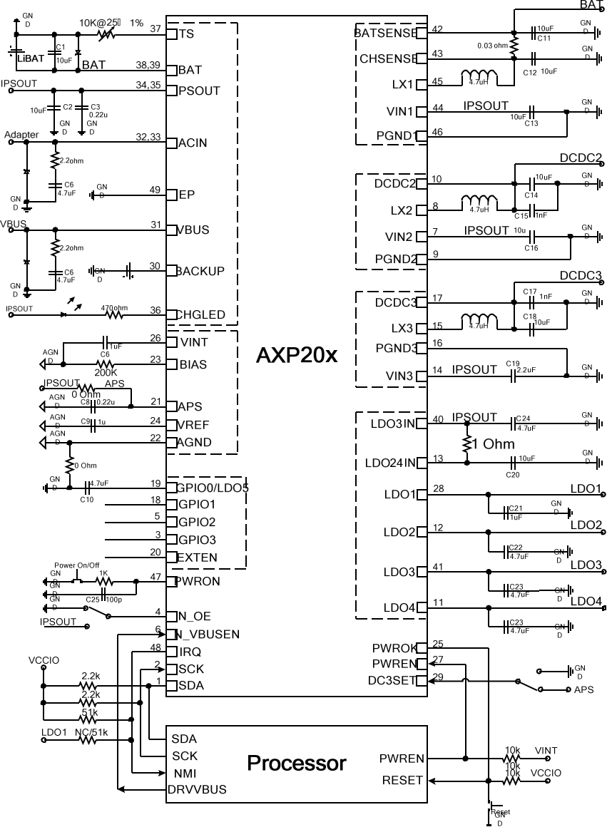
More hints are provided in our self-translated V3s Hardware Design Guide (page 7) too.
PMIC Schematics
The FunKey S device uses all of the U5 AXP209 integrated SMPS:
- the PWM charger DC-DC1 for the battery
- the DC-DC2 for providing the +1.25 V / 1.6A to the core
- the DC-DC3 for providing the +3.3V / 1.2A to the I/Os
But compared to the sophisticated reference design above, the FunKey S device only uses 2 out of the 5 integrated LDOs:
- LDO1 supplies the +3.3V / 30 mA Always On for the RTC
- LDO2 provides the +3.0V / 200 mA for the analog power supply
- LDO3 / LDO4 / LDO5 are not used in the FunKey S
Here are the PMIC schematics:
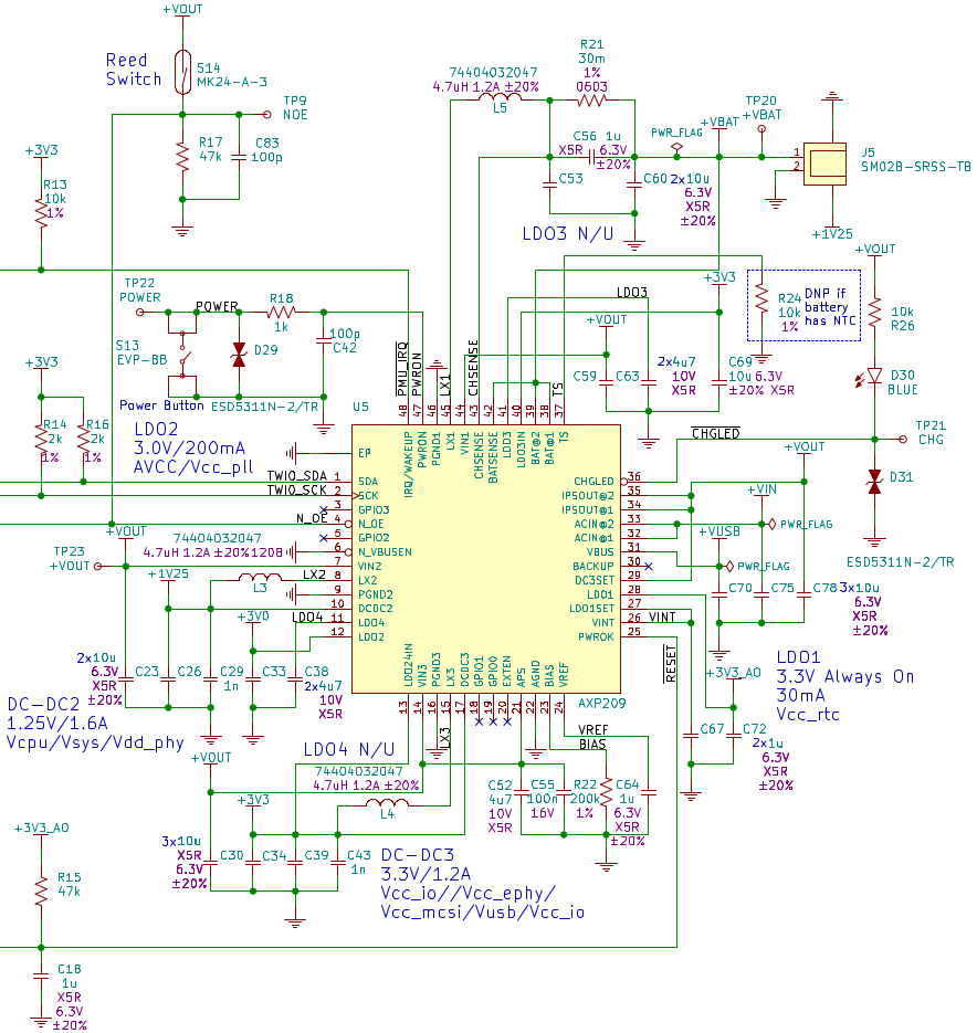
These schematics may look intimidating and complex, but they are in fact just a collection of simple basic elements, and it is actually very close to the manufacturer-recommended design.
Here are the details for each PMIC functions, one by one:
Power Inputs (East side)
A wall-plug AC adapter input is not used in the FunKey S device, so +VIN is just filtered using C75 on pins 32 and 33.
The USB power input +VUSB on pin 31 is filtered using C70, and the best (between +VUSB and +VBAT) available voltage is output to +VOUT on pins 34 and 35 and filtered using C78.
The BACKUP supply on pin 30 is not used and is left unconnected.
Internal Connections (All sides)
Some AXP20x signals are externally available and should be connected to external components:
-
The BIAS connection on pin 23 is connected to a precision 200k 1% resistor R22, as recommended
-
The reference voltage VREF on pin 24 is decoupled with C64
-
The +2.5V internal logic voltage VINT on pin 26 is filtered using the recommended value for C67
Additionally, the AXP20x is actually made up of separate flexible blocks that require external interconnections to set their desired operation:
-
All DC/DC inputs (VIN1 on pin 44, VIN2 on pin 7 and VIN3 on pin 14), as well as LDO3IN input on pin 40 are connected to the best available voltage +VOUT with filter capacitors C59, C23, C30, and C69, respectively
-
LDO1SET on pin 27 is used to set the initial voltage of LDO1, and according to the datasheets, setting it to VINT sets its voltage to the desired +3.3V for the +3.3V Always On power supply
-
OTOH, combined LDO 2 and 4 input LDOIN24 on pin 13 is instead connected to +3.3V in order to minimize the voltage drop for LDO2 to generate the +3.0V. Here too, there is a filter capacitor C34
-
It is not clear what is the exact function of APS on pin 21 (it is described as "Internal Power Input"), but it must be connected to +VOUT, too
DC-DC1 PWM Battery Charger (North East side)
The battery is connected to J5 (a 2-pin JST 1.0 mm pitch receptacle) and uses R21 as a precision current sense resistor, with C53/C56/C60 filter capacitors and L5 (a low-profile ferrite-core power inductor rated with a saturation current of 1.2A and low < 0.1 Ω resistance).
Warning
The battery is not protected on the board against reversing polarity, as the model used already contains a built-in protection.
R24 is mounted to simulate a battery NTC resistor for measuring temperature, as the chosen LiPo battery does not feature this temperature sensor.
A user-programmable (through the I2C interface) charge LED D30 is provided, with its current-limiting resistor R26, as well as a TVS diode d31 to prevent ESD, as the LED body will be indirectly accessible to user.
DC-DC2 +1.25V / 1.6A (West side)
This SMPS is built around the ferrite core power inductor L3 and filter capacitors C26 and C29.
DC-DC3 +3.3V / 1.2A (South side)
This SMPS is built around the ferrite core power inductor L4 and filter capacitors C39 and C43.
LDO1 +3.3V Always On 30mA (South East side)
The LDO output on pin 28 is filtered with capacitor C72.
LDO2 +3.0V / 200mA (South West side)
The LDO output on pin 12 is filtered with capacitor C33.
LDO3 (North side)
This LDO is not used and its output on pin 41 is nevertheless filtered with a capacitor C63.
LDO4 (South West side)
This LDO is not used and its output on pin 11 is nevertheless filtered with a capacitor C38.
Power Key (North West side)
The AXP20x features a soft power key with internal short and long-press detection with user-programmable time settings, which enables turning power ON or OFF much like the way it is done in cellular phones.
Only a few external components are required: the tactile switch S13, its ESD protection TVS D29, and a low-pass filter R18 and C42 for debouncing the switch.
I2C Bus (North West side)
The AXP20x can be externally controlled by the main CPU using the I2C bus on pins 1 and 2. This bus has pull-up resistors to +3.3V R14 and R16, and the IRQ/WAKEUP signal on pin 48 enables warning or waking up the CPU on a selection of AXP20x-generated events, with a pull-up resistor R13 to +3.3V.
GPIOs (South and West sides)
GPIO0-3 on pins 19, 18, 5 and 3 are not used in the FunKey S and are left unconnected.
PWROK (South West side)
The PWROK signal on pin 25 is used to generate the global RESET signal for the whole board, with a pull-up resistor R15 to the +3.3V Always On power supply and a filter capacitor C18.
Enable Signals (West side)
The global chip enable signal N_OE on pin 4 is activated by default through a 47kΩ resistor R17 to GND, but a magnetic Reed switch S14 can disable it by forcing its level to +VOUT, with a filter capacitor C83. This circuit will be disscused later in the Magnetic Switch section.
The USB enable signal N_VBUSEN on pin 6 is directly tied to GND to always enable power from the USB bus.
Monitoring
Through the I2C bus and the numerous internal available registers, the AXP20x provides a very fine control of its operation, including many threshold and timing settings, but also many voltage and curent monitoring values.
Coulomb Counters / Fuel Gauge
It is well known that battery discharge voltage curve over time is very flat, making it very difficult to estimate the real charge/discharge state of the battery. Moreover, this state will vary with temperature, load, and aging.
The only accurate way to monitor the battery status is to actually count the energy that is stored when charging, and the one that is consumed. This particularly important feature is achieved in the AXP20x using a dual Coulomb counter which continuously sums the current intensity over time for monitoring the battery accurate charge and discharge status, with user-defined alert thresholds.
This fuel gauge is providing the ability to precisely report the remaining battery capacity, just like people are used to with cellular phones.