DRAM Power
A separate Sylergy SY8088 Buck DC/DC SMPS chip is used to provide the DDR2 +1V8 DDR2 DRAM power.
This is because the AXP20x is originally the PMU (Power Management Unit) used by most Allwinner SoCs (A10, A13 and A20), which do not integrate SDRAM, so the board designer has a wide choice of memory option: DDR2, DDR3, DDR3L, LPDDR3, LPDDR4 with various voltage requirements.
But no specific PMIC was created for the Allwinner V3s used in the FunKey device which however integrates a fixed SiP (System In Package) 512Mbit (64MB) DDR2 SDRAM.
We thus have to design a separate SMPS (DC-DC) power supply for providing the +1.8V 1A required for the DDR2 DRAM power supply.
For this purpose, we followed closely the Allwinner Reference Design.
Here is the corresponding DRAM Power schematics:
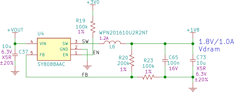
Nothing very fancy here: the SMPS chip U4 has its required input filter capacitor C37 and output capacitors C65 and C73.
The low-profile ferrite-core power inductor L6 (rated with a saturation current of 1.76A and low < 0.1 Ω resistance) provides the DC-DC energy storage element.
The R20/R23 precision voltage divider provides the required +0.6V feedback voltage from the +1.8V output voltage by having a ⅓ resistor ratio.
The last component is a pull-up resistor R19 which ties the SMPS chip enable input to its active level permanently. The pull-up voltage is +3.0V (just as in the original reference design), probably as it is the next higher voltage available, in order to limit the current in it to its lowest possible value.