CPU
The main part in the FunKey S device is of course its CPU.
As discussed in the Design Constraints section, a CPU with external DRAM chips would take too much real-estate on the PCB, so we had to find a CPU with integrated DRAM.
There are several options for integrating RAM in a SoC:
-
use SRAM: not possible because of the small amount of memory available (64Mbit max.)
-
embedded DRAM on the same chip: This is the solution used in the Apple M1 chip, but this chip is not available for retail and no other solutions seems readily available
-
Stacked Chip-on-Chip (PoP): This is the solution used on some Raspberry Pi boards, but this solution is only available for custom designs, with minimum order quantities not compatible with the FunKey S low volumes
-
DRAM die in SiP: with capacities ranging from 64Mbit to 1Gbit
We found only 2 manufacturers providing the last option: Microchip and Allwinner Technology. Microchip solutions are too limited in term of CPU power for our needs (ARM926EJ-S or Cortex A5), so we did not consider them.
And with the exception of the mostly similar Allwinner S3 CPU which features the same characteristics but with 128MB DDR3 DRAM in an FBGA234 package, the Allwinner V3s is the CPU with integrated DRAM having the highest memory capacity (512Mbit / 64MB DDR2 DRAM):
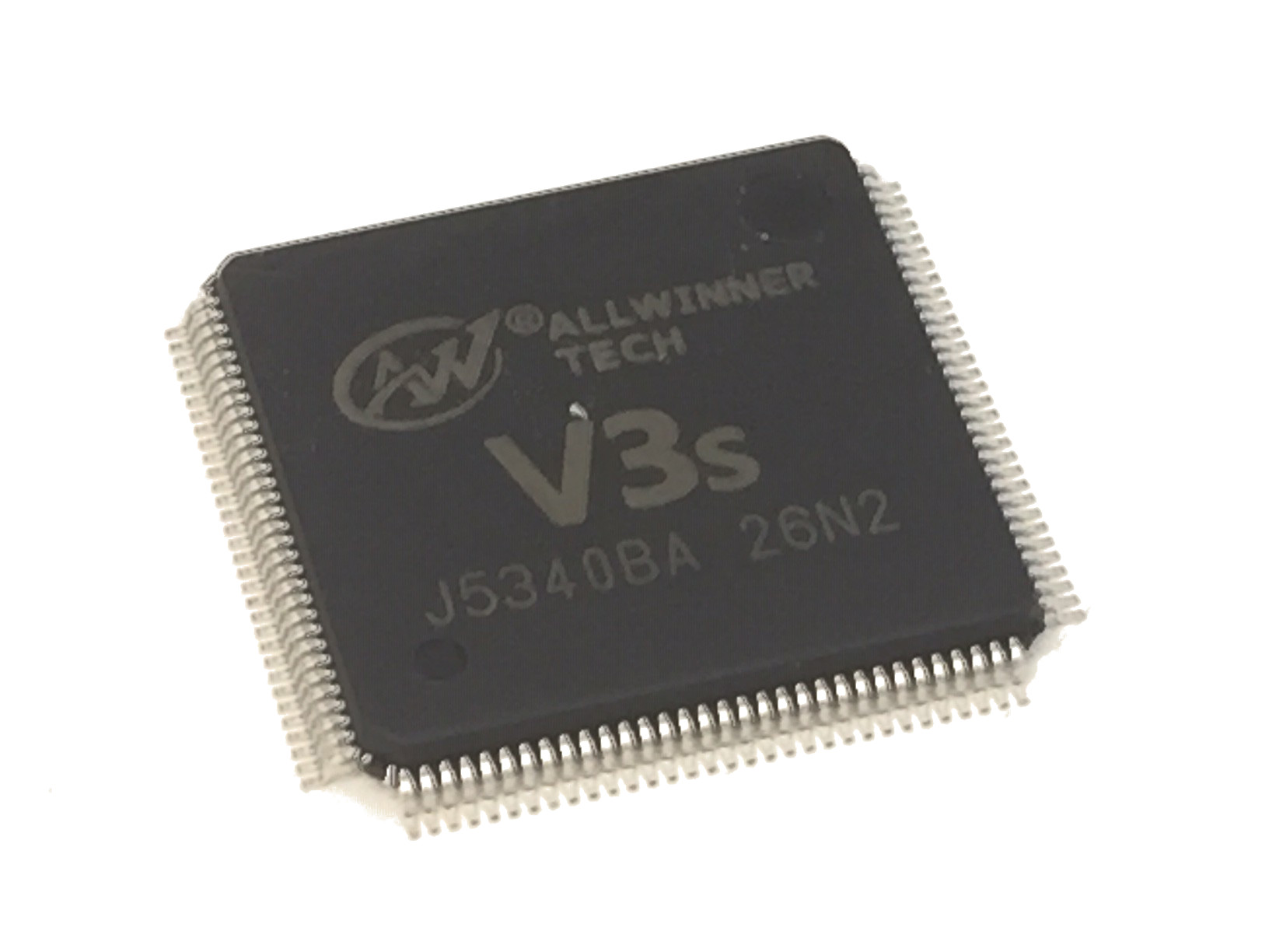
Despite its larger package size (16mm x 16mm vs. 11mm x 11mm), we selected the V3s over the S3 because of its better availability and ease of soldering of the LQFP128 over the FBGA234 package for the prototypes.
The V3s features a rather powerful single-core ARM Cortex A7-A clocked @ 1.2GHz with an additional Vector Floating Point Version 4 (vfpv4) FPU extension and an SIMD NEON architecture with a 32 × 64-bit register file and 64-bit ALU, but unfortunately no GPU or 2D graphic engine containing a hardware scaler that could be extremely useful for the retro-gaming emulators.
As a bonus, as the V3s is based on an ARM Cortex A7-A low-power architecture, it also features a low power consumption which is required by our battery operation.
These characteristics do not look very impressive compared to a Raspberry Pi for example, but using many optimizations and after running many tests, we found them nevertheless satisfactory for our purpose.
CPU Schematics
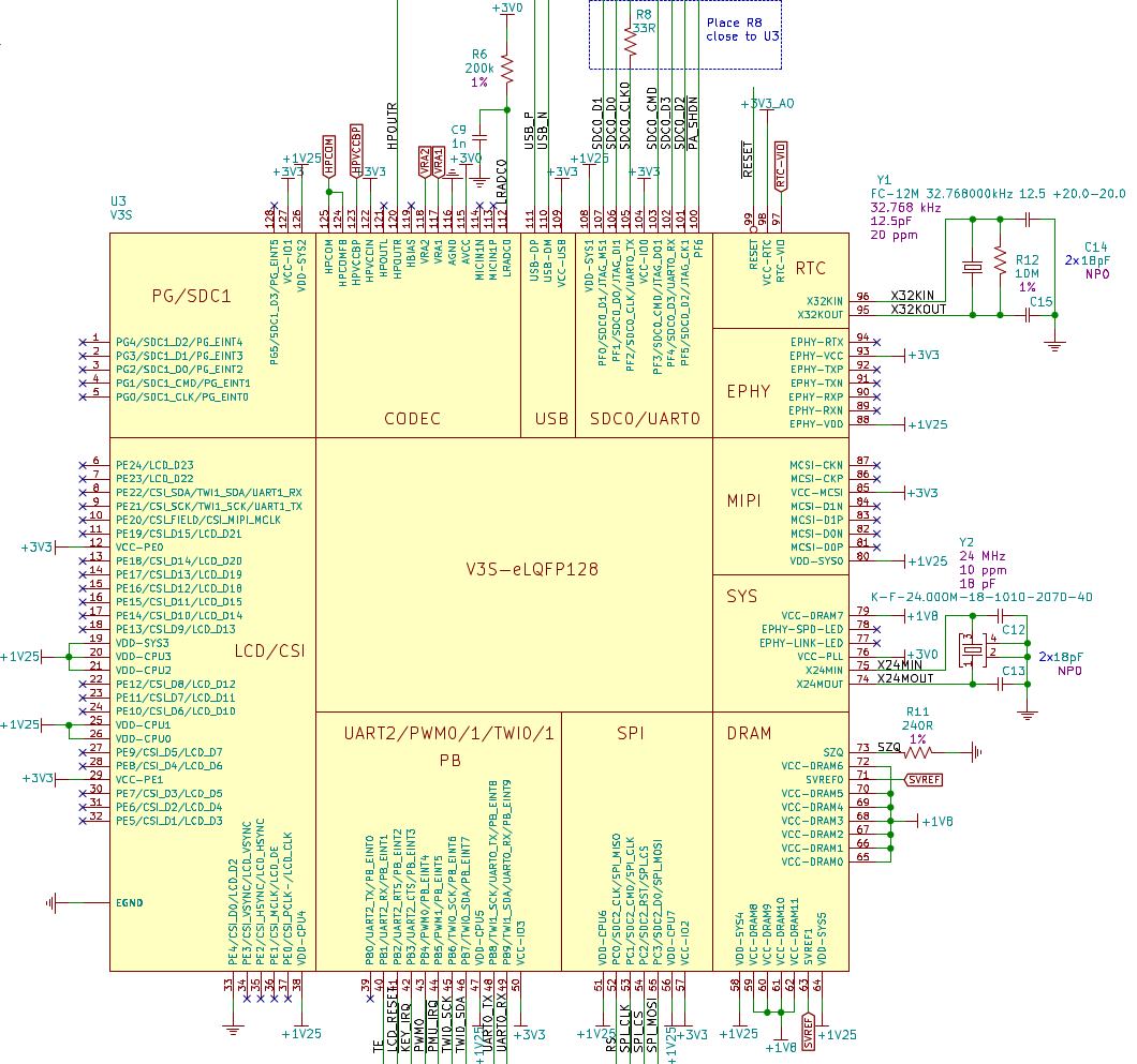
Here is the part of the schematics corresponding to the CPU core:
SoC Blocks
As can be seen, there is not much besides the CPU chip U3 itself... The CPU is in fact a SoC (System on Chip) containing a collection of built-in peripheral and memory blocks along with the CPU itself:
-
the LCD / DSi display peripheral
-
the GPIO port G / SDC1 (SD Card #1) interface
-
the AUDIO codec
-
the LRADC0 (Low-Resolution Analog to Digital Converter)
-
the USB OTG controller
-
the GPIO port F / SDC0 (SD Card #0) / UART0 interface
-
the RTC (Real Time Clock) timer
-
the EPHY (Ethernet PHYsical) interface
-
the MIPI CSi camera interface
-
the built-in 64 MB DDR2 DRAM
-
the GPIO port C / SPI interface
-
the GPIO port B / UART2 / PWM0 / PWM1 / TWI0 (I2C #0) / TWI1 (I2C #1)
Among these, the FunKey device only uses a few blocks:
-
AUDIO
-
USB (as device only)
-
SDC0 (for SD Card)
-
RTC
-
DRAM
-
SPI (for the LCD screen)
-
PWM0 (for backlight)
-
TWI0 (for I2C bus to control the GPIO expander and power management chips)
-
A couple of GPIOs to power the audio power amplifier and get feedback interrupt signals from the the GPIO expander and power management chips
CPU Power Supplies
What is remarkable though is that the V3s requires a lot of different voltages for its power supply:
- +3V3 for the I/O power supply
- +3V3_AO for the Always-On power supply (RTC timer)
- +3V0 for analog power supply
- +1V8 for the DDR2 DRAM power supply
- +1V25 for the core power supply
This profusion of different power supplies as well as the high power drawn by some of them (1.2A for +3V3, 1.6A for +1.25V) requires a sophisticated power management that will be detailed further.
LRADC0
The LRADC0 (Low-Resolution Analog to Digital Converter #0) is designed to measure the voltage of a resistor ladder switched by keyboard keys: this single input is thus in theory able to manage a keyboard of up to 10 keys @ 250 Hz.
Unfortunately, the FunKey has 12 keys (U/D/L/R, A/B/X/Y, RR/RL, Start and Fn), and the resulting key detection accuracy is not compatible with a gaming usage because of long term stability problems. This is the reason why it is not used in the FunKey and just terminated by a proper low-pass filter R6/C9 to avoid picking up noise glitches.
SD Card
The SD Card interface is almost a direct connection between the chip and the dedicated SD Card connector. Only a single series resistor R8 is required on the high-speed clock line in order to prevent ringing.
Crystals
The V3s chips requires 2 crystals:
-
one low-frequency 32.768 kHz crystal Y1 for the RTC clock
-
one high-frequency 24 MHz crystal Y2 for deriving the 1.2 GHz clock
The 24 MHz crystal is used by an internal oscillator to lock the phase of the 1.2 GHz oscillator using a PLL (Phase-Locked Loop).
The 32.768 kHz crystal is used by another internal oscillator to tick the RTC (Real-Time Clock) at a standard watch frequency.
These crystals require 2 load capacitors each (C12/C13 and C14/C15 respectively) in order to guarantee that the oscillators still start and work with a comfortable operation margin taking into account voltage, temperature and aging.
The 32.768 kHz crystal features an additional high-value resistor R12 in order to limit the internal oscillator's output current and thus reduce further the RTC timer power consumption.
For more details on crystal oscillator design, please check this application note from STM.
DRAM
The DRAM within the V3s chip is a DDR2 one, meaning that its data lines are clocked using both edges of an up to 400 MHz clock signal.
At these high frequencies, even short wires have a length that is of the same order of magnitude as the signal's wavelength and thus each signal should be considered as a transmission line, for which impedance must be matched to avoid signal reflections, requiring termination resistors on the data lines DQx.
DDR2 or DDR3 DRAMs feature merged drivers and dynamic on-chip termination like this ("VDDQ/2" is labeled "SVREF" in our schematic):
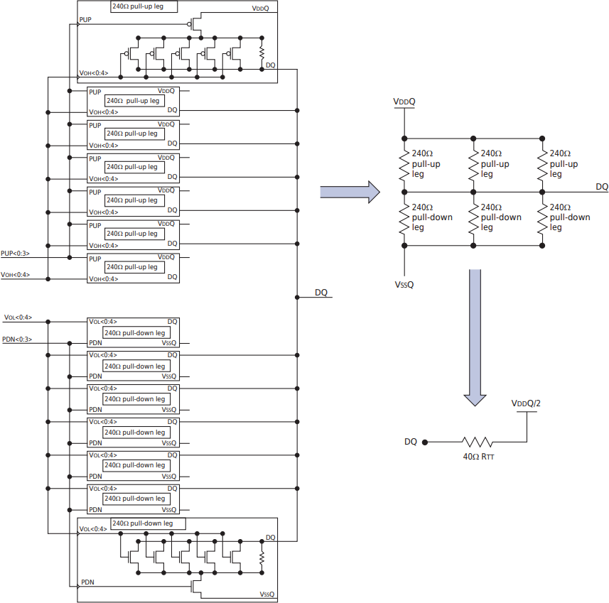
The V3s DDR2 DRAM has an active termination calibration circuitry and procedure called "ZQ Calibration" requiring an accurate 1% 240 Ω resistor R11 connected internally like this:
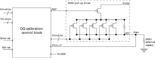
More information on the DDR2 DRAM ZQ Calibration subject can be found in this Micron Application Note.