Buttons
As a generic game console emulating many classic ones, the FunKey requires numerous buttons:
- A soft "ON/OFF" button
- A "+" control pad with "Up", "Down", "Left" and "Right" buttons
- A "X" control pad with "A", "B", "X" and "Y" buttons
- "Start" and a "Fn" buttons
- At least L1 and R1 shoulder buttons
As can be seen in the page on the PMIC, the soft "ON/OFF" button is directly connected to the power management chip, so we are left with 4 + 4 + 2 = 12 buttons for game control.
After testing tactile domes in our FunKey Zero prototype, we decided to go back to integrated tactile switches, as their placement is much easier using a regular SMT pick & place machine like any other components on the PCB, whereas the separate tactile domes required an adhesive tape to be place manually with less accuracy.
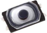
The Mitsumi BYS-055A1x12 is the same footprint (2.5mm x 1.6mm x 0.55mm) as the more expensive Panasonic EVBBBxAAB00 tactile switches, with a 1.2N actuating force for the "+" and "X" pads, and a 1.6N actuating force for the "Start", "Fn" and "ON/OFF" buttons. We found these actuating force the best match to provide a good feedback to the user.
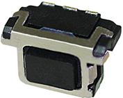
For the rear left and right shoulder buttons, we exeperimented several models between PCBA rev. C, D and E, until we eventually decided for a replacement for the expensive Panasonic EVP-AEBB2A-1:
This one as an actuating force of 1.6N.
GPIO Requirements
The Allwinner v3s CPU comes in a large 128-pin TQFP package, with a lot of exposed (51!) GPIO pins:
- PB0 to PB9 (10)
- PC0 to PC3 (4)
- PE0 to PE24 (25)
- PF0 to PF5 (6)
- PG0 to PG5 (6)
The FunKey specializes some of them for specific interfaces like SDCard, PWM, SPI and I2C buses, console UART, but most of them are left available for I/Os.
GPIO Expander
But for the FunKey S device and given the small PCB size, wiring all the buttons directly to the V3s puts a lot of constraints on the PCB routing, at such a point that we decided to use a dedicated I2C GPIO expander chip to relieve the burden from the main V3s CPU.
We use a common chip for this purpose, that is well supported in the Linux kernel: the NXP PCAL6416AHF.128. It is marketed as a "low-voltage translating 16-bit I2C-bus/SMBus I/O expander with interrupt output, reset, and configuration registers" that just matches exactly our needs.
As a bonus, this chip features software-controlable internal pull-up/pull-down resistors, so we don't need to add external ones to fix the defaut button states.
The connection with the V3s CPU is achieved using standard I2C clock (SCL) and data (SDA) signals, plus an additional IRQ signal driven by the I/O expander when pre-programmed conditions are met, such as a key press / release event. A RESET signal is used to initialize the chip when required.
Schematics
Here is the corresponding main schematic for the buttons:
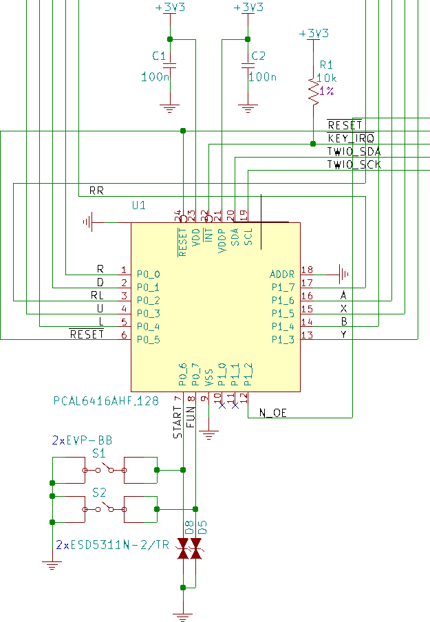
The main component is of course the I/O expander U1, with the control signals to the CPU/PMIC on the north side.
The chip's /INT signal is pulled up to the +3V3 power supply by the resistor R1, such that the active-low interrupt signal is disabled by default.
The I/O expander chip features 2 separate power supplies VDD and VDDP for the core and peripheral respectively, each decoupled by a bulk capacitor C1 and C2.
Except for the GPIO I/Os, the only remaining pin is the ADDR pin 18 which provides the I2C address LSB bit, so that you can address 2 PCAL6416AHF.128 chips on the same I2C bus by wiring this pin differently.
Tip
One oddity is that the pin 6 (P0_5) is connected to the /RESET signal: it is a routing trick to get this signal to go through this pin pad, as it was very difficult to access it otherwise...
The "Start" and "Select" buttons S1 and S2 are 2 low-profile SMT tactile switches, each featuring an ESD protection TVS diode D8 and D5, as these buttons are of course accessible by the user!
The other buttons are wired in the same fashion:
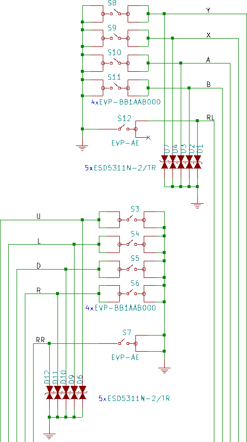
The "U", "L", "D", "R", "A", "B", "X" and "Y" buttons S3, S4, S5, S6, S8, S9, S10 and S11 are of the same kind and also have a respective TVS diodes D2, D3, D4, D5, D6, D7, D8, D9, D10 and D11.
The left (S12) and right (S7) shoulder buttons are right angle SMT tactile buttons, with their TVS diode D1 and D12.
Benefit
The main advantage of this solutions is that the 12 signals to wire the buttons to the CPU are replaced by only 4 signals, from which 3 are shared with the other I2C peripherals (the PMIC) on the bus.
It is then much easier to route this dense PCB by delegating the button GPIO handling to a satellite chip.