Architecture
Block Diagram
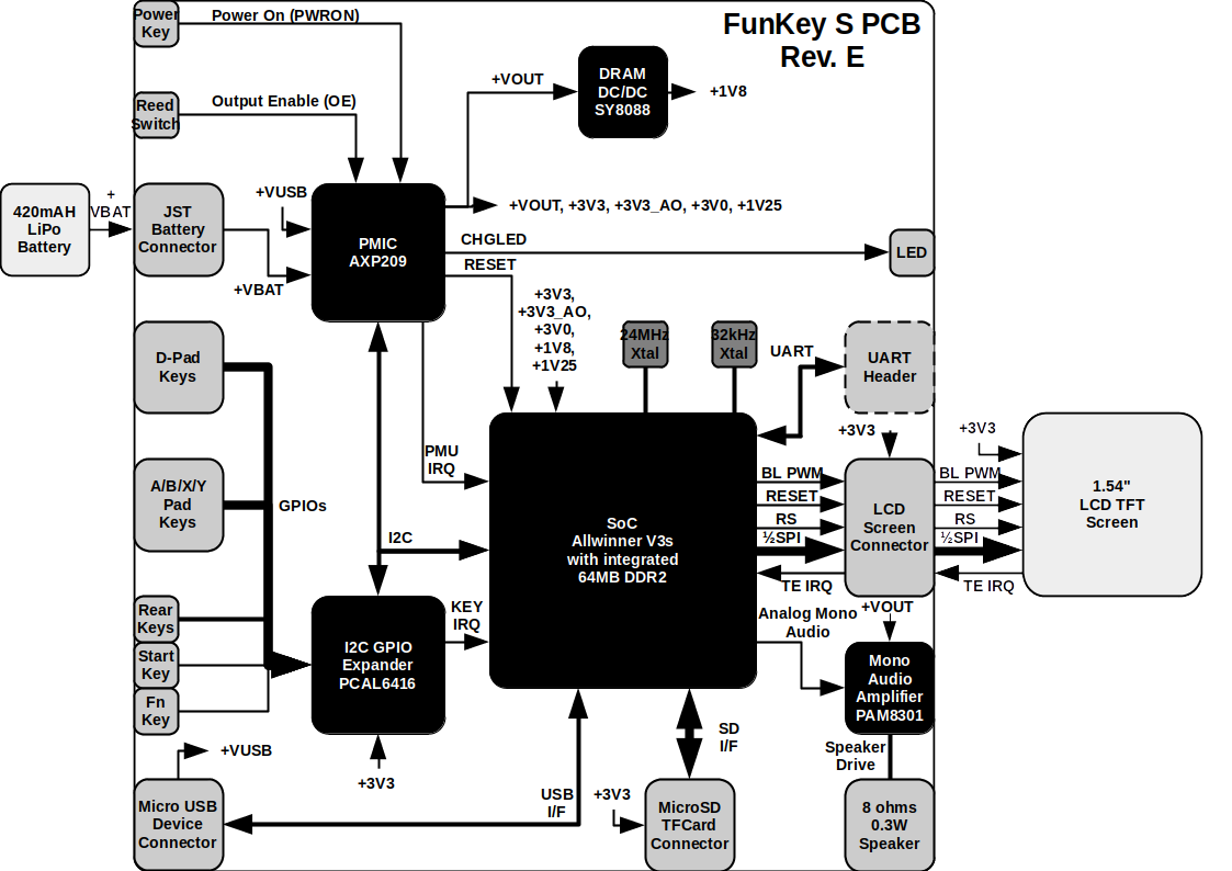
Eventually, the design constraints listed in the previous section led to the following electronic diagram, featuring 3 main blocks:
-
1x main PCB (0.8 mm thickness) with components on both sides, the maximum component height above PCB on both sides is 1.5 mm. Current revision for this board is Revision E
-
1x 1.54” IPS TFT LCD screen with SPI interface and using a custom flex cable, containing a built-in screen controller chip
-
1x 420 mAh 402540 LiPo battery, containing an active protection circuitry
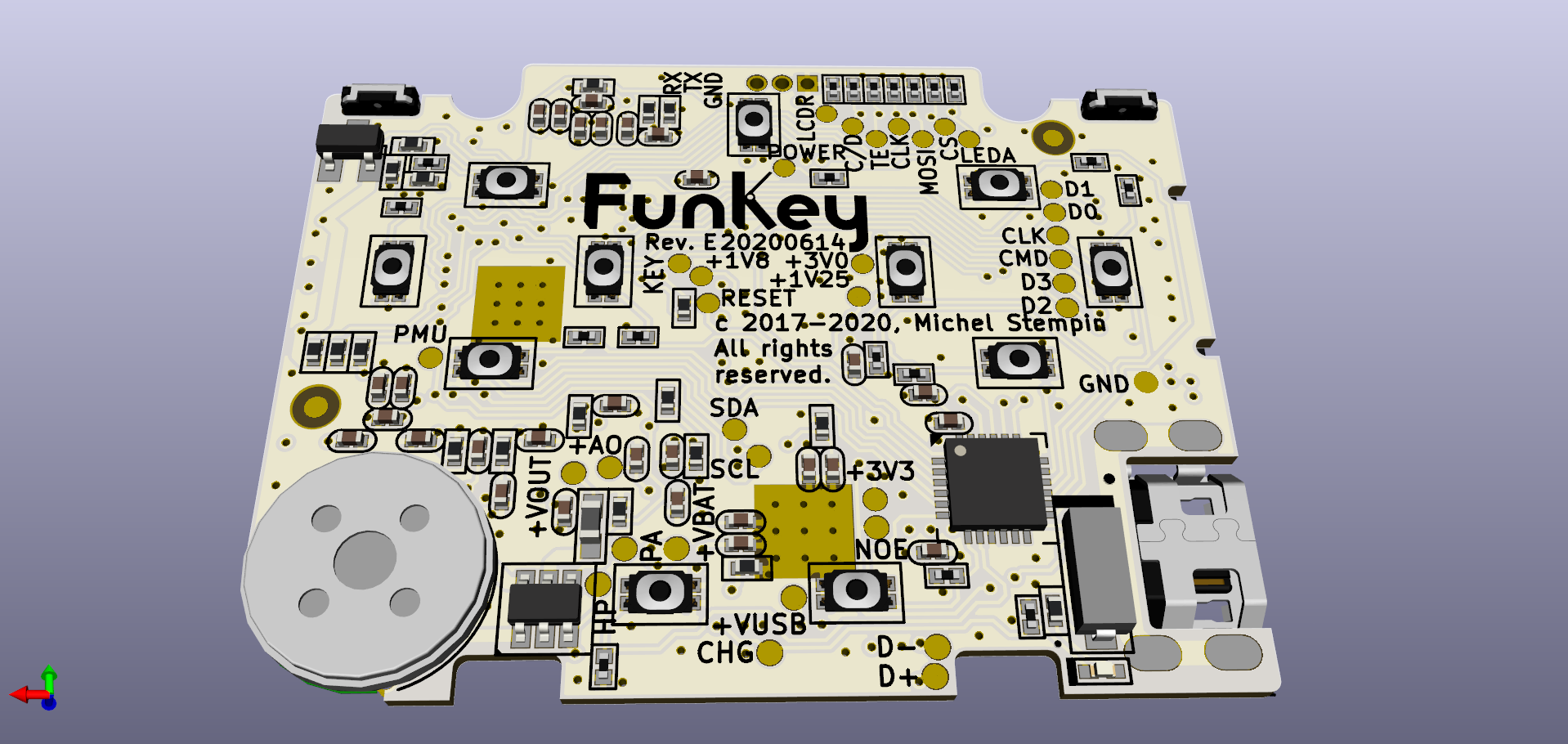
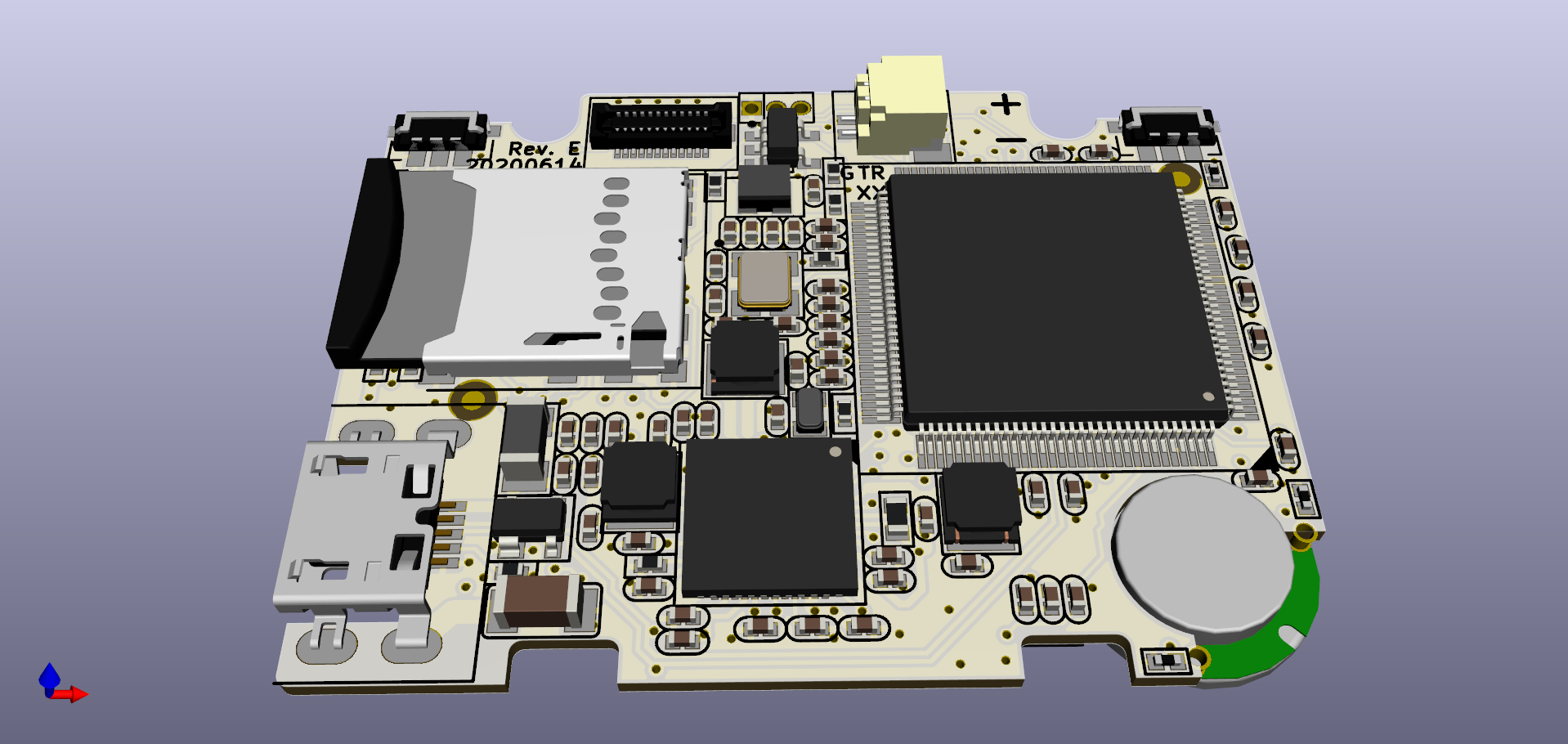
3D View
A 3D rendering of the PCBA done in KiCAD produces the images below:
BOM
An interactive BOM is available in the next section.
Schematics and Layout
All the hardware design and production files required to build the FunKey S retro-gaming console electronic PCBA using the KiCAD ECAD tools are available as Open Hardware in the FunKey S Hardware repository.
Topological vs. logical schematic symbols
The FunKey S schematics use symbols and placement that are as close as possible to their corresponding physical package and layout, instead of defining symbols that are conveniently arranged by logical properties. Even if this makes schematics more complex at first sight, the benefit of this approach is that the step to go from the schematics to the physical layout becomes much easier, and so is the debugging of the physical board, which is then very close to the schematics too.
Explicit schematic wires
Another habit that is used everywhere in the FunKey S schematics is that all signals (except power supplies and GND) are routed using explicit wires, rather than counting on invisible connection by net names and relying of the reader to search these names all over the place. This forces related components to be clustered in compact groups to shorten the wires, and put more focus on inter-cluster signals, with a natural inclination to unravel wire nests in the schematics before laying out the actual board.
Power supply nets
There are some "PWR_FLAG" symbols added here and there, which is the proper way in KiCAD to declare that a given net has a known supply and thus prevent the ERC (Electrical Rule Check) to throw an error.
The schematics will be discussed function by function in the following sections.